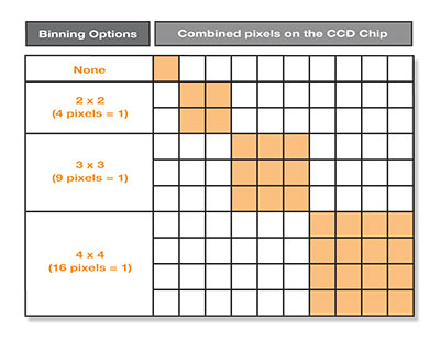
CCD Binning or Pixel Binning
CCD Binning (or Pixel Binning) is the process of combining neighboring pixels on an image sensor (CCD sensor) into a “super pixel”. This super pixel represents the area of all the individual pixels contributing to the charge. For example, in 2 x 2 CCD binning, the charge from a square of 4 adjacent pixels is combined into 1, and in 3 x 3 CCD binning, the charge from a square of 9 adjacent pixels is combined into 1.

Binning provides several beneficial results: 1) An increase in signal equal to the number of pixels binned. This allows the camera to detect fainter signals and reduce exposure time. 2) An increase in frame rate due to the reduction in exposure time and a reduction in the number of pixels to be measured 3) An increase in the signal to noise ratio resulting from a single read error being applied to the charge of the binned pixels rather than the addition of multiple read errors if the pixels were read individually. 4) An increase in the dynamic range of the sensor resulting from the larger charge capacity of the summing node (typically 1.65-2 times increase in well depth).
The trade off for the gains due to binning are: 1) A loss of image resolution equal to the binning level. 2) An increase in dark current proportional to the number of pixels binned.

